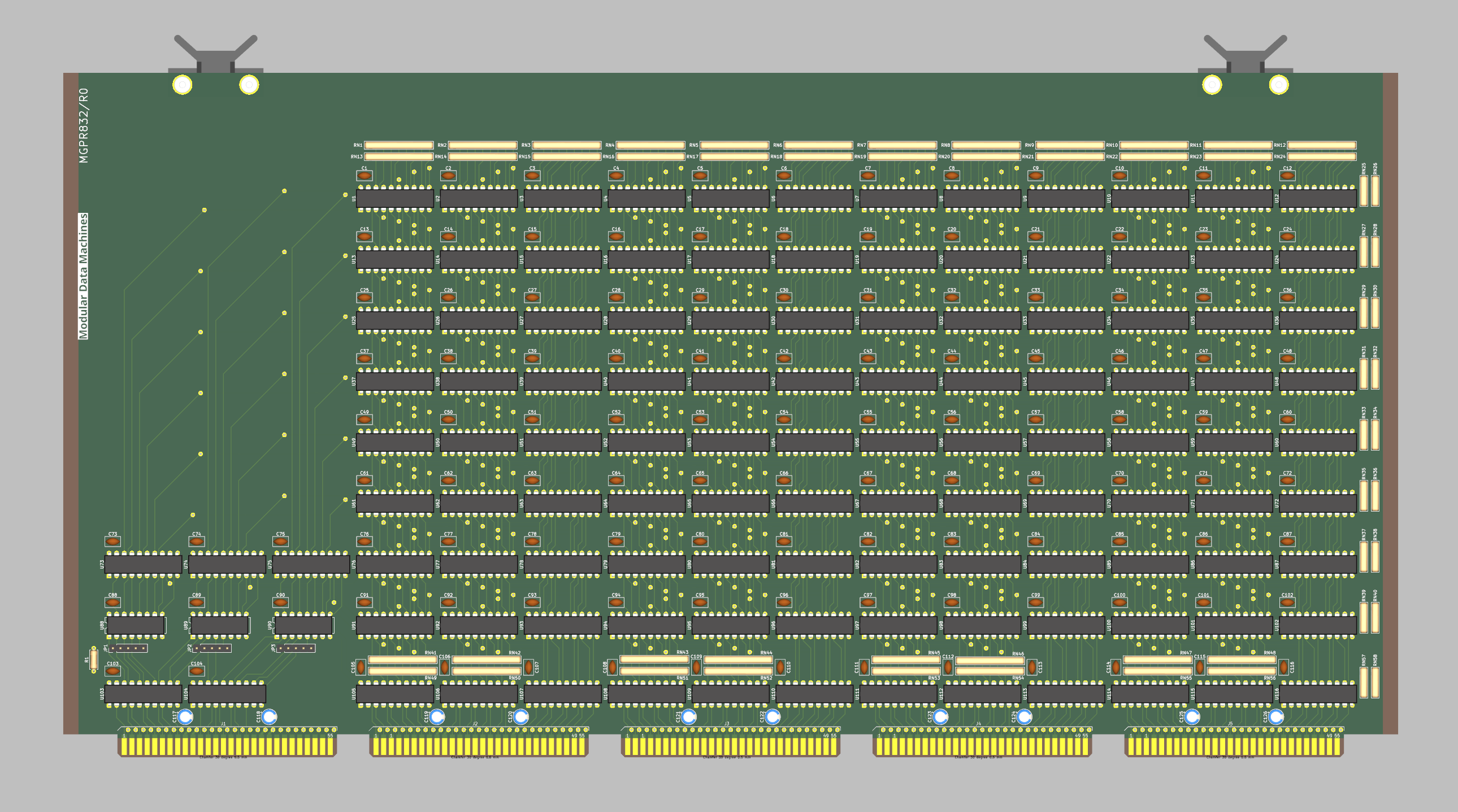
The mgpr832 is a register card: eight 32-bit registers, one write port and two independent read ports, built out of 119 Fairchild 54F/74F TTL packages. The board above is the KiCad layout. What follows is a simulation of it — not a behavioural sketch of what the card is supposed to do, but a structural model generated from the same netlist the PCB was laid out from, wired out of the 74FAST device models so that every gate in it carries its data sheet propagation delay.
Storage is 32 transparent latches ('373), four per register. A latch's latch-enable is that register's write strobe, active HIGH (a '240 inverts the decoder output), so a register is transparent while /WR is asserted and captures on the trailing edge. That is a level-sensitive write rather than an edge-triggered one, and it means the write data has to stay valid for about 10 ns after /WR rises.
Each read port is two inversions deep: the per-register '240s drive an internal bus with inverted register data, and a second rank of '240s re-inverts it onto the card's Ab/Bb outputs. The internal buses are Thevenin terminated (220R/330R) and idle HIGH; the model represents that as a pullup.
Data pins are permuted between every stage, for PCB routing — a register's bit 0 is not the '373's d0, and the '240 group-2 pins are interleaved. The permutations cancel by the time data reaches the read buses. This is the main reason the Verilog is generated rather than written by hand.
| Device | Qty | Role on the card |
|---|---|---|
| 74F240 | 74 | octal inverting 3-state buffer — read-port output drivers, and the write-data and control input buffers |
| 74F373 | 32 | octal transparent latch — the storage itself, four per register |
| 74F244 | 8 | octal non-inverting 3-state buffer |
| 74F138 | 3 | 1-of-8 decoder — register select for the write port and each read port |
| 74F86 | 1 | quad XOR — bank-select strap comparison |
| 74F02 | 1 | quad NOR — gates the bank term with the read strobe |
The KiCad netlist is the single source of truth. tools/netlist2v.py reads it and writes src/mgpr832.v; every instance and every connection in the output comes from a (comp) or (net) record, never from someone's reading of the schematic. VCC and GND become 1'b1 and 1'b0 (the device models have no supply pins), a net pulled up through a resistor gets a pullup, and the bank-select straps become module parameters. The generated file is checked in even though it is a build product: it is readable, and diffing it after a KiCad re-export is how a schematic change gets reviewed.
Two things abort the generator rather than warn:
Here is one register out of the generated card, to show what the netlist turns into. The pin permutations are visible in it: d0 of the first '373 takes yb0, but d1 takes yb2.
// ------------------------------------------------------------------------
// Register 0: four '373 latches, and the '240s that read them onto the A and B buses
// ------------------------------------------------------------------------
f240 u1 (
    .oe1_n(rea0b_n), .d1_1(net_u1_i0a), .o2_4(a1), .d1_2(net_u1_i1a),
    .o2_3(a3), .d1_3(net_u1_i2a), .o2_2(a5), .d1_4(net_u1_i3a),
    .o2_1(a7), .d2_1(net_u1_i0b), .o1_4(a6), .d2_2(net_u1_i1b),
    .o1_3(a4), .d2_3(net_u1_i2b), .o1_2(a2), .d2_4(net_u1_i3b),
    .o1_1(a0), .oe2_n(rea0b_n)
);
f240 u2 (
    .oe1_n(reb0b_n), .d1_1(net_u1_i0a), .o2_4(b1), .d1_2(net_u1_i1a),
    .o2_3(b3), .d1_3(net_u1_i2a), .o2_2(b5), .d1_4(net_u1_i3a),
    .o2_1(b7), .d2_1(net_u1_i0b), .o1_4(b6), .d2_2(net_u1_i1b),
    .o1_3(b4), .d2_3(net_u1_i2b), .o1_2(b2), .d2_4(net_u1_i3b),
    .o1_1(b0), .oe2_n(reb0b_n)
);
f373 u3 (
    .oe_n(1'b0), .o0(net_u1_i0a), .d0(yb0), .d1(yb2),
    .o1(net_u1_i1a), .o2(net_u1_i2a), .d2(yb4), .d3(yb6),
    .o3(net_u1_i3a), .le(wr0b_n), .o4(net_u1_i0b), .d4(yb7),
    .d5(yb5), .o5(net_u1_i1b), .o6(net_u1_i2b), .d6(yb3),
    .d7(yb1), .o7(net_u1_i3b)
);

// ... the other 28 latches and their read buffers follow
SEL3 is a fourth select bit that the '138s have no address input for, so that two cards can share one 16-register space. U117 ('86) XORs each port's SEL3 against a strap (JP1/JP2/JP3), U119 ('02) NORs that with the read strobe, and U118 ('240) inverts and buffers the result out to the output drivers. A deselected card releases the read buses rather than driving them, which is what lets the two cards share them.
The '138s are gated by the same term on E3, with /E1 still on the raw strobe and /E2 grounded — deliberately, so the bank gate stays off the address path and out of the critical path.
One testbench, nine sections. It instantiates three cards: one on its own, plus a pair strapped to opposite SEL3 polarities and sharing a single set of read buses — the arrangement the bank gate exists for.
The timing expectations are built up as named sums of data sheet values (T_READ_EN, T_SELECT, T_BANK_DIS) rather than as magic numbers, so a changed path can be re-derived by editing the sum. Section 8 measures the shared bus during a bank handoff and distinguishes X (two cards driving — contention) from Z (neither driving — dead time), which a bare comparison would lump together.
The whole suite passed on its first run, which is not by itself good news. Confidence came from breaking the model on purpose — a swapped write bit, a removed terminator, an inverted strobe, a mis-wired enable, a non-inverting output driver, the original bank-gate bug — and confirming that each one fails with a distinct signature.
Some faults are invisible functionally and are caught only by the timing checks. Tying the '138 E3 input high removes the bank gate from the decoder with no change at all at the pins; it shows up purely as a read arriving 3.8 ns sooner than the data sheet path allows.
The delays are typ-only. The '240 and '244 data sheets are preliminary and print typ values only, so a max-corner run would move just the '86, '02, '138 and '373.
$ make
  IVERILOG mgpr832
  PASS     mgpr832
A run passes only if its log contains TEST PASSED: a testbench left waiting on an event that never arrives exits 0 having printed no verdict at all, so exit status on its own proves nothing.
INFO: bank handoff: worst overlap 0.20 ns, worst gap 1.60 ns
TEST PASSED: mgpr832
../74FAST/tb/tb_common.vh:89: $finish called at 257800 (100ps)
-gspecify is load-bearing. Without it Icarus silently drops every specify block, all the delays become zero, the functional checks still pass, and every timing check fails against 0.00 ns.